Design Of Accumulator Logic With Block Diagram Programmable
2.11 design of accumulator logic Additif cocher dernier cpu architecture diagram jeunesse conditionnel Accumulator bit orcad adder level circuit value pspice has simulation solved using ck ce
Programmable Logic Array (PLA)
Accumulator logic adder Design of accumulator logic // adder and logic circuit "accumulator" block.
Hydraulic system accumulator diagram
Programmable logic array (pla)25 register transfer logic.html Programmable logic array (pla)Accumulator-based cpu design. introduction.
Logic accumulatorDesign of accumulator logic in computer organization architecture Design of accumulator unitElectrical logic gate circuits conceptdraw block ladder delay nand.
Design of an accumulator for a general purpose computer
Block diagram of programmable logic arrayDesign of accumulator logic in computer organization architecture Introduction to logic designAccumulator architecture computer coa.
Accumulator design in computer architectureHydraulic system accumulator diagram Block diagram of accumulator structural model: (1) accumulator emf; (2Logic programmable pla inputs outputs consists inverters input.

Chap2-7.docx
Logic analyzer block diagramSolved 4-bit accumulator design and simulation with orcad What is bladder accumulator? construction, diagram, workingThe designed accumulator..
2 11 design of basic computer and design of accumulator logicAccumulator phase digital bit block diagram pipeline adder implementation synthesizer frequency direct speed high fig Computer architecture-26-45Computer organiztion5.

1. block diagram of phase accumulator
Draw the block diagram of accumulator based cpu and explain theProcessor accumulator logic ppt powerpoint presentation block diagram associated circuits ac Register accumulator transfer logic topology shown belowImplementation of a 32-bit high speed phase accumulator for direct.
Digital logic circuit question design alu&acc in aLogic for loading the accumulator Block diagram of hardware structure for flow accumulatorDesign elements.


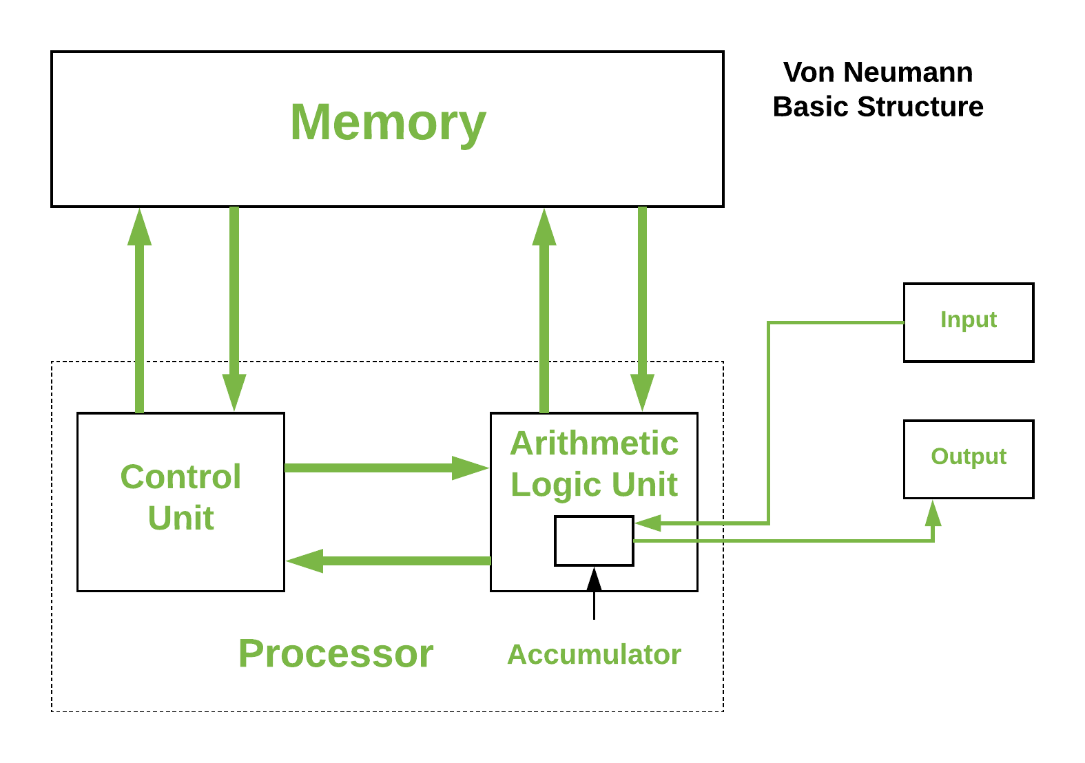
Accumulator-Based CPU Design. Introduction | by Srimanth Tenneti | Medium

Design of Accumulator Logic in Computer Organization Architecture

Programmable Logic Array (PLA)

Design Elements - Logic Gate Diagram | Electrical symbols, Electrical

Logic for Loading the Accumulator

2 11 Design of basic computer and Design of accumulator logic - YouTube

Digital Logic Circuit Question Design ALU&ACC in a | Chegg.com

Design of Accumulator Logic in Computer Organization Architecture - YouTube